SN74AUP1T32,pdf(Low Power, 1.8
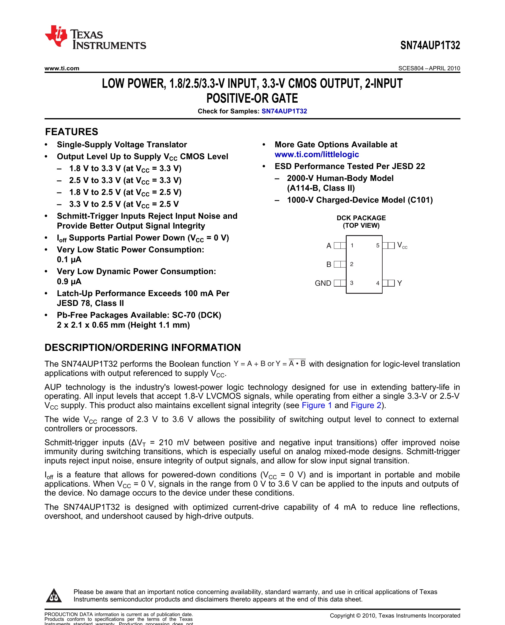
The SN74AUP1T32 performs the Boolean funcTIon Y = A + B or Y = A\ • B\ with designaTIon for logic-level translaTIon applicaTIons with output referenced to supply VCC.
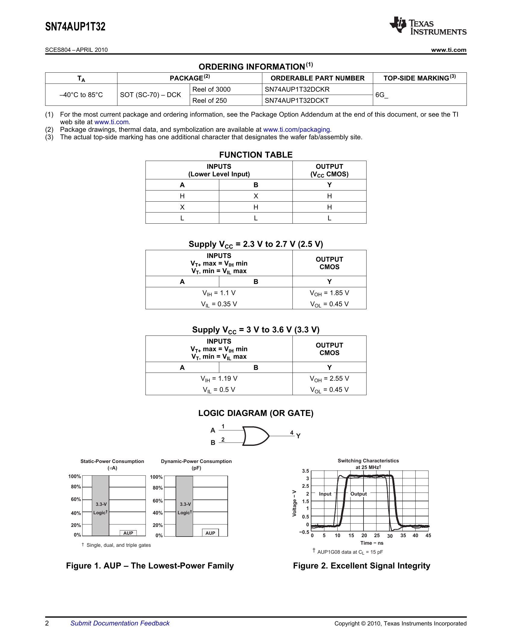
AUP technology is the industry’s lowest-power logic technology designed for use in extending battery-life in operating. All input levels that accept 1.8-V LVCMOS signals, while operating from either a single 3.3-V or 2.5-V VCC supply. This product also maintains excellent signal integrity (see Figure 1 and Figure 2).
The wide VCC range of 2.3 V to 3.6 V allows the possibility of switching output level to connect to external controllers or processors.
Ioff is a feature that allows for powered-down conditions (VCC = 0 V) and is important in portable and mobile applications. When VCC = 0 V, signals in the range from 0 V to 3.6 V can be applied to the inputs and outputs of the device. No damage occurs to the device under these conditions.
The SN74AUP1T32 is designed with optimized current-drive capability of 4 mA to reduce line reflections, overshoot, and undershoot caused by high-drive outputs.


